You are using an out of date browser. It may not display this or other websites correctly.
You should upgrade or use an alternative browser.
You should upgrade or use an alternative browser.
DJI Phantom 2 Vision FC200 EGG camera - Black video FPV solution to fix
- Thread starter masterphantom
- Start date
Thank you quaddamage
i will probably need a different USB-TTL, i think I have it here around otherwise I will order it on Amazon.
My first concern, now, is to weld wires on those four tiny service pads!
is your camera functional, is there some hope that you ll be able to strip the firmware?
thank you!
For BTSEL (Boot Select) pad - here is a post which seem to identify it, almost correctly:
 phantompilots.com
Almost - bacause it suggests to connect to bottom terminal of the registor, and I'm pretty sure that's ground. I think upper terminal is the BTSEL.
lightbridge firmware PROBLEM (and solution) - firmware version not found by dji assistant tool
I got the know how from the following site GitHub - mefistotelis/phantom-firmware-tools: Tools for handling DJI Phantom quadcopter firmwares. Here is what I did to flash the DM36x . To enter boot mode I connected 1 & 2 to 3.3v. My ftdi did not provide enough current to boot the board. Used...
Almost - bacause it suggests to connect to bottom terminal of the registor, and I'm pretty sure that's ground. I think upper terminal is the BTSEL.
[/QUOTE]
Quaddamage, I am far from an electronics engineer.....do you know if there is anyone or a company that will fix the issue like mine with the FC200....everything works except for FPV, and that began years ago after DJI pushed an update for the firmware(s). TIA.No idea how this is news for anyone.. we can fix DaVincis for like 4 years now. There are lots of threads and external articles on that:
The most relevant threads:
lightbridge firmware PROBLEM (and solution) - firmware version not found by dji assistant tool
This thread is becomed a little bit too long to be read. for anyone interested just in the solution, I pasted here directly the conclusions. UPDATE: if you send Lightbridge to me I can repair it for 45€. If you have any problem with the procedure or if you want to go deep in how I found the...phantompilots.com
Articles:PV2+ no live feed
Hello all new here .great fourms ! .. Ok here is the million dollar question ? After countless weeks of Searching boards everywhere has any one actually found a fix to this issue ? I've done everything there possibly could be done other than take it apart .trust me I've done every trial an error...phantompilots.com
This one even mentions FC200 directly:
DJI Phantom 2 Vision+ Plus Blank Screen Corrupt NAND fix
Contact For questions, feedback or repair service inquiries, please find my contact details here: http://scr.im/okstuv For a great video walk-through of this repair process, check out this great YouTube video made by FlyMyMavic: Let's Begin This brief tutorial aims to help people fix the blacksites.google.com
Flashing firmware on DaVinci media processors
And here's another one which I made, for the situations when NAND chip needs replacing:
Fixing flash in DM365 chip within Ph3 Pro gimbal
Here is a success story I wanted to share. I had a Phantom 3 Pro gimbal which didn't allowed me to see the FPV feed. Photos and movies were recorded on sd-card, there was just no live video - only grey background - in Dji Go. I explained the details, and the road to fixing the issue, here...phantompilots.com
Sure, we don't have complete firmwares for all of the boards - but reflashing bootloader we can do on all of them.
Quaddamage, I am far from an electronics engineer.....do you know if there is anyone or a company that will fix the issue like mine with the FC200
In Poland, there are both electronic repair stores which handle all devices, and specialized stores which repair drones. No idea for other countries.
I have limited experience with that; I fix my things myself.
Hi quaddamage, i'm in...
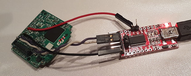
...and nothing happens in Putty.
So i think i am in that condition:
2. Nothing happens. Still only cursor on screen.
In this case we can't be sure whether the DM36x doesn't print anything (which indicates bootloader damage), or your serial connection is broken somehow.
Your setup, you need to test by yourself. Maybe RX and TX wires are switched? Maybe your USB-to-TTL just doesn't work? If there's no apparent issue, you can just assume it's bootloader damage. While fixing it, you will have another opportunity to test the serial setup.
To fix bootloader damage - go to "Re-flashing bootloader" chapter below.
so, i have to try to:
Re-flashing bootloader
To re-flash bootloader, you first need to force the chip into serial programming mode. This will make the chip ignore content of NAND memory, and instead wait for commands on serial interface. To enter serial programming mode, solder the Boot Select service pad BTSEL to 3.3V pad.
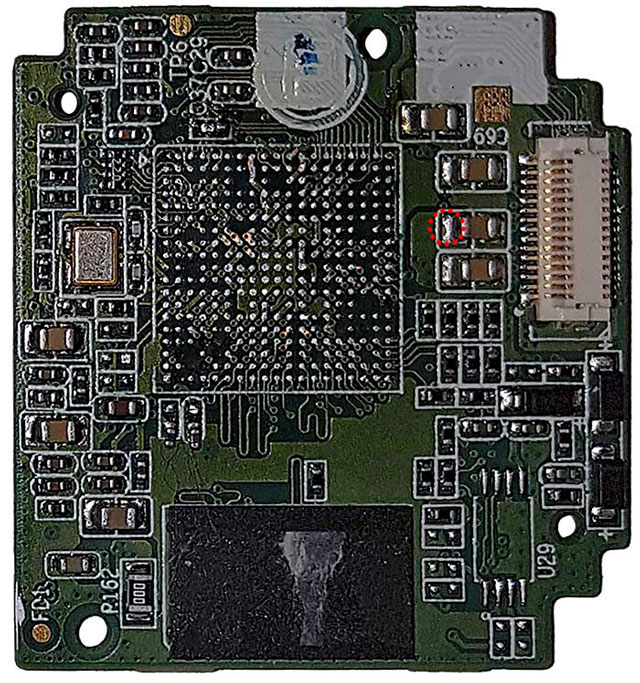
Please quaddamage, can you confirm i have to solder 3.3V to the red circle in this picture?
thank you
...and nothing happens in Putty.
So i think i am in that condition:
2. Nothing happens. Still only cursor on screen.
In this case we can't be sure whether the DM36x doesn't print anything (which indicates bootloader damage), or your serial connection is broken somehow.
Your setup, you need to test by yourself. Maybe RX and TX wires are switched? Maybe your USB-to-TTL just doesn't work? If there's no apparent issue, you can just assume it's bootloader damage. While fixing it, you will have another opportunity to test the serial setup.
To fix bootloader damage - go to "Re-flashing bootloader" chapter below.
so, i have to try to:
Re-flashing bootloader
To re-flash bootloader, you first need to force the chip into serial programming mode. This will make the chip ignore content of NAND memory, and instead wait for commands on serial interface. To enter serial programming mode, solder the Boot Select service pad BTSEL to 3.3V pad.
Please quaddamage, can you confirm i have to solder 3.3V to the red circle in this picture?
thank you
NO! Don't solder 3.3V to that capacitor!
Who gave you that idea!? that's clearly a power rail.
You have 3 capacitors there. Below, there is a row of 4 resistors. And below that, is a row of 3 resistors.
You probably need to solder 3.3V to the middle resistor of these 3. Or left and middle.
These resistors are clearly a pull down resistors, meaning they are connected to the chips BTSEL on one side, and to GND on the other side. Make sure you're not shorting 3.3V to the ground - solder it on proper side. Measure resistance to ground to check which side is proper.
Explanation:
In documentation which you can download from Texas Instruments, titled: "TMS320DM365 Digital Media System-on-Chip (DMSoC)", there's boot modes explanation, ie:
So normally the chip boots from NAND - meaning we can assume all BTSEL pins are pulled down to ground through resistors (mode BTSEL[2:0] = 000 from the documentation). To enter serial (UART) boot mode and be able to flash the bootloader, we need to change that to BTSEL[2:0] = 011. So we need to change two bits to logical "1" - which is 3.3V.
Now, where are those connections on the image of the chip? The TI documentation states that too:

So as you see, the logical value of BTSEL is taken from pins/pads named EM_A[13:11]. We are interested in EM_A[12] and EM_A[11] only. And here is where they are on the footprint:
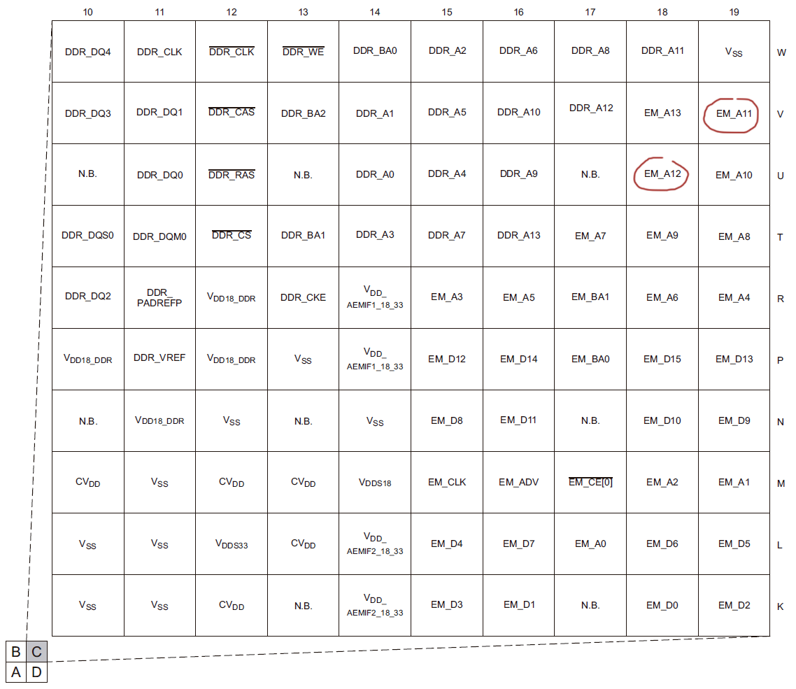
The image is explained as "Pin Map (Bottom View)" - which means it needs to be flipped to match the footprint on the photo. The board photo you pasted has pin 1 marked in top left, and if we flip the image around horizonal line, we will get the same orientation. Our culpit pads are:
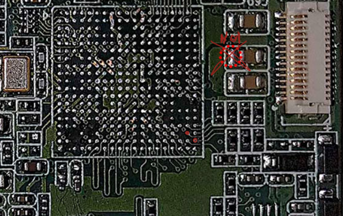
It looks to me that these pads got to the top of the first two resistors in the 3-resistor line. Though in the thread I linked, someone said only the 2nd resistor matters, and he soldered to its bottom.. that is suspicious. He might have made a short circuit, and entered the flashing mode by pure luck. To make sure, I'd use a multimeter. Check for zero resistance to GND.
Who gave you that idea!? that's clearly a power rail.
You have 3 capacitors there. Below, there is a row of 4 resistors. And below that, is a row of 3 resistors.
You probably need to solder 3.3V to the middle resistor of these 3. Or left and middle.
These resistors are clearly a pull down resistors, meaning they are connected to the chips BTSEL on one side, and to GND on the other side. Make sure you're not shorting 3.3V to the ground - solder it on proper side. Measure resistance to ground to check which side is proper.
Explanation:
In documentation which you can download from Texas Instruments, titled: "TMS320DM365 Digital Media System-on-Chip (DMSoC)", there's boot modes explanation, ie:
• If BTSEL[2:0] = 001 - Asynchronous EMIF boot mode [...]
• The RBL (boot loader stored internally in the chip) supports 7 distinct boot modes:
– BTSEL[2:0] = 000 - NAND Boot mode
– BTSEL[2:0] = 010 - MMC0/SD0 Boot mode
– BTSEL[2:0] = 011 - UART0 Boot mode
– BTSEL[2:0] = 100 - USB Boot mode
– BTSEL[2:0] = 101 - SPI0 Boot mode
– BTSEL[2:0] = 110 - EMAC Boot mode
– BTSEL[2:0] = 111 - HPI Boot mode
So normally the chip boots from NAND - meaning we can assume all BTSEL pins are pulled down to ground through resistors (mode BTSEL[2:0] = 000 from the documentation). To enter serial (UART) boot mode and be able to flash the bootloader, we need to change that to BTSEL[2:0] = 011. So we need to change two bits to logical "1" - which is 3.3V.
Now, where are those connections on the image of the chip? The TI documentation states that too:
So as you see, the logical value of BTSEL is taken from pins/pads named EM_A[13:11]. We are interested in EM_A[12] and EM_A[11] only. And here is where they are on the footprint:
The image is explained as "Pin Map (Bottom View)" - which means it needs to be flipped to match the footprint on the photo. The board photo you pasted has pin 1 marked in top left, and if we flip the image around horizonal line, we will get the same orientation. Our culpit pads are:
It looks to me that these pads got to the top of the first two resistors in the 3-resistor line. Though in the thread I linked, someone said only the 2nd resistor matters, and he soldered to its bottom.. that is suspicious. He might have made a short circuit, and entered the flashing mode by pure luck. To make sure, I'd use a multimeter. Check for zero resistance to GND.
Last edited:
NO! Don't solder 3.3V to that capacitor!
Who gave you that idea!? that's clearly a power rail.
I was confusing capacitors and resistors ... what a shame! ?
You have 3 capacitors there. Below, there is a row of 4 resistors. And below that, is a row of 3 resistors.
You probably need to solder 3.3V to the middle resistor of these 3. Or left and middle.
These resistors are clearly a pull down resistors, meaning they are connected to the chips BTSEL on one side, and to GND on the other side. Make sure you're not shorting 3.3V to the ground - solder it on proper side. Measure resistance to ground to check which side is proper.
It looks to me that these pads got to the top of the first two resistors in the 3-resistor line. Though in the thread I linked, someone said only the 2nd resistor matters, and he soldered to its bottom.. that is suspicious. He might have made a short circuit, and entered the flashing mode by pure luck. To make sure, I'd use a multimeter. Check for zero resistance to GND.
I checked with my multimeter and i'm pretty sure that only the bottom of the first resistor has zero resistance to GND:
so, maybe, only the FIRST resistor matters?
lightbridge firmware PROBLEM (and solution) - firmware version not found by dji assistant tool
I got the know how from the following site GitHub - mefistotelis/phantom-firmware-tools: Tools for handling DJI Phantom quadcopter firmwares. Here is what I did to flash the DM36x . To enter boot mode I connected 1 & 2 to 3.3v. My ftdi did not provide enough current to boot the board. Used...
so, maybe, only the FIRST resistor matters?
Hard to tell exactly.. one of the pads we need to connect clearly goes to first resistor. The other goes under the white paint, so it's hard to tell. Maybe these two are connected, and so the solution which PriEgor just re-posted is the correct one.
lightbridge firmware PROBLEM (and solution) - firmware version not found by dji assistant tool
I got the know how from the following site GitHub - mefistotelis/phantom-firmware-tools: Tools for handling DJI Phantom quadcopter firmwares. Here is what I did to flash the DM36x . To enter boot mode I connected 1 & 2 to 3.3v. My ftdi did not provide enough current to boot the board. Used...phantompilots.com
Hallo PriEgor, thank you for help. And quaddamage too, of course.
But now i'm a little confused about the procedure to force the chip into serial programming mode...
1) so we just need a short (temporary) contact from TP10 to the resistor descibed in picture one https://phantompilots.com/attachments/20170905_143426-jpg.87846/ to make when I already have the Putty serial window open?
2) or we need a contact between 3.3v and the middle resistor shown in picture two https://phantompilots.com/attachments/20170905_143455-jpg.87847/? a temporary or continuous contact?
3) or we need both?
Thank you again for your patience
All the connections you make are temporary. It's up to you where you use 3.3V from - TP10 is one possibility.so we just need a short (temporary) contact from TP10 to the resistor descibed in picture one
Changing the value of BTSEL bits only has effect during chip boot. After that, it doesn't do anything. Anything good and anything bad.when I already have the Putty serial window open?
If it affects power consumption or resets the board, you're just making a short circuit.
Putty window is linked to your USB-to-TTL, not to the target board.
Hi guys
i connected the middle resistor shown by PriEgor to the TP10 pad, but still nothing new from Putty...
But checking the circuit i noticed some oddities, because from TP3 GND:
at TP10 i have 0,6V inste3ad of 3,3V
at TP4 i have 0V instead of 1,2V
at TP7 i have 0,7V instead 1,8V
at TP8 i have 0,9V instead of 3V
Doesn't sound very good huh?
Can i try taking 3.3V from USB-to-TTL instead of TP10?
Maybe better to take 5V and GND from external power instead of USB-to-TTL?
Maybe better to take 5V and GND from external power instead of USB-to-TTL?
Yes, that's a correct conclusion - your USB clearly can't power the chip, this is why it doesn't work.
When working with Ph3, I used 1A USB out. Though it had to power Ambarella as well - for you the draw shouldn't be that high.
Yes, that's a correct conclusion - your USB clearly can't power the chip, this is why it doesn't work.
When working with Ph3, I used 1A USB out. Though it had to power Ambarella as well - for you the draw shouldn't be that high.
First i diconnected TP10 from resistor, to restart from beginning.
But even using a 5V 6A external power instread of USB-to-TTL I get a low voltage on the pads mentioned above (very strange, it would seems even lower than before!)
But, making numerous different attempts i realized that if i connect +5V and GND before (from external or from USB-TTL too), and then only after i connect the TX RX wires i get a "connected" status with some garbage text in Putty window.
The TTL logic is set to 3.3V (the jumper is on the middle and the 3.3V pins); maybe i have to try different serial settings, i.e. lower speed than 115200?
i get a "connected" status with some garbage text in Putty window.
[...] maybe i have to try different serial settings, i.e. lower speed than 115200?
If you see garbage which does not resemble text - then yes, the issue is with connection parameters: baud rate, bit count, stop bits etc.
quaddamage, i was wrong from the beginning ... 
DM365 chip is the same of your tutorial but the FC200 Live View Encoder board don't need 5v to power on, it only needs GND to TP3 and 3V to TP8
This is my Putty log:
DM36x initialization passed!
TI UBL Version: 1.50
Booting Catalog Boot Loader
BootMode = NAND
Starting NAND Copy...
Valid magicnum, 0xA1ACED66, found in block 0x00000019.
DM36x initialization passed!
TI UBL Version: 1.50
Booting Catalog Boot Loader
BootMode = NAND
Starting NAND Copy...
Valid magicnum, 0xA1ACED66, found in block 0x00000019.
DM36x initialization passed!
TI UBL Version: 1.50
Booting Catalog Boot Loader
BootMode = NAND
Starting NAND Copy...
Valid magicnum, 0xA1ACED66, found in block 0x00000019.
DM36x initialization passed!
TI UBL Version: 1.50
Booting Catalog Boot Loader
BootMode = NAND
Starting NAND Copy...
Valid magicnum,DM36x initialization passed!
TI UBL Version: 1.50
Booting Catalog Boot Loader
BootMode = NAND
Starting NAND Copy...
Valid mDM36x initialization passed!
TI UBL Version: 1.50
Booting Catalog Boot Loader
BootMode = NAND
Starting NAND Copy...
Valid mDM36x initialization passed!
TI UBL Version: 1.50
Booting Catalog Boot Loader
BootMode = NAND
Starting NAND Copy...
Valid magicnum, 0xA1ACED66, found in block 0x00000019.
DM36x initialization passed!
TI UBL Version: 1.50
Booting Catalog Boot Loader
BootMode = NAND
Starting NAND Copy...
Valid magicnum, 0xA1ACED66, found in block 0x00000019.
DM36x initialization passed!
TI UBL Version: 1.50
Booting Catalog Boot Loader
BootMode = NAND
Starting NAND Copy...
Valid magDM36x initialization passed!
TI UBL Version: 1.50
Booting Catalog Boot Loader
BootMode = NAND
Starting NAND Copy...
ValiDM36x initialization passed!
TI UBL Version: 1.50
Booting Catalog Boot Loader
BootMode = NAND
Starting NAND Copy...
Valid magicnum, 0xA1ACED66, found in block 0x00000019.
DM36x initialization passed!
TI UBL Version: 1.50
Booting Catalog Boot Loader
BootMode = NAND
Starting NAND Copy...
Valid magicnum, 0xA1ACED66, found in block 0x00000019.
What do you think about it?
I need to reflash the bootloader, or other actions that i can do?
Well, it is clear that the chip constantly restarts. And it restarts before it tries to boot kernel:
So it looks like the issue is with bootloader.
Code:
DM36x initialization passed!
TI UBL Version: 1.50
Booting Catalog Boot Loader
BootMode = NAND
Starting NAND Copy...
Valid magicnum, 0xA1ACED66, found in block 0x00000019.
(chip reset)
So it looks like the issue is with bootloader.
hello experts
I have a problem with my wifi module from a ph2 V+. I flashed many wifi boards for my friends without problems. the board is also correct connected...
now I have a board which I can flash but it will not work.. I have a error lines:
NAND block 0xxxxxxxx is bad!!!
Is it possible to fix this fail?
thanks for answer....
flashing log:
log in teraterm after flashing:
I have a problem with my wifi module from a ph2 V+. I flashed many wifi boards for my friends without problems. the board is also correct connected...
now I have a board which I can flash but it will not work.. I have a error lines:
NAND block 0xxxxxxxx is bad!!!
Is it possible to fix this fail?
thanks for answer....
flashing log:
Code:
-----------------------------------------------------
   TI Serial Flasher Host Program for DM36x
   (C) 2009, Texas Instruments, Inc.
   Ver. 1.50
-----------------------------------------------------


Flashing NAND with ubl1_editedByGaucho.img and u-boot_modifiedByGaucho.img.


Attempting to connect to device COM3...
Press any key to end this program at any time.


Waiting for the DM36x...
        Target:  BOOTME
BOOTME commmand received. Returning ACK and header...
ACK command sent. Waiting for BEGIN command...
        Target:   BEGIN
BEGIN commmand received. Sending CRC table...
 100% [                                                              ]
                           CRC table sent....


Waiting for DONE...
        Target:    DONE
DONE received.  Sending the UBL...
 100% [                                                              ]
                              UBL sent....


        Target:    DONE
DONE received.  UBL was accepted.
UBL transmitted successfully.


Waiting for SFT on the DM36x...
        Target: Starting UART Boot...
        Target: BOOTUBL
BOOTUBL commmand received. Returning CMD and command...
CMD value sent.  Waiting for DONE...
        Target:    DONE
DONE received. Command was accepted.
Sending the UBL image
Waiting for SENDIMG sequence...
        Target: SENDIMG
SENDIMG received. Returning ACK and header for image data...
ACK command sent. Waiting for BEGIN command...
        Target:   BEGIN
BEGIN commmand received.
 100% [                                                              ]
                           Image data sent...


Waiting for DONE...
        Target:    DONE
DONE received.  All bytes of image data received...
        Target: Writing UBL to NAND flash
        Target: Unprotecting blocks 0x00000001 through 0x00000018.
        Target: Number of blocks needed for header and data: 0x0x00000001
        Target: NAND block 0x00000001 is bad!!!
        Target: NAND block 0x00000002 is bad!!!
        Target: NAND block 0x00000003 is bad!!!
        Target: NAND block 0x00000004 is bad!!!
        Target: NAND block 0x00000005 is bad!!!
        Target: NAND block 0x00000006 is bad!!!
        Target: NAND block 0x00000007 is bad!!!
        Target: NAND block 0x00000008 is bad!!!
        Target: NAND block 0x00000009 is bad!!!
        Target: NAND block 0x0000000A is bad!!!
        Target: NAND block 0x0000000B is bad!!!
        Target: NAND block 0x0000000C is bad!!!
        Target: NAND block 0x0000000D is bad!!!
        Target: NAND block 0x0000000E is bad!!!
        Target: NAND block 0x0000000F is bad!!!
        Target: NAND block 0x00000010 is bad!!!
        Target: NAND block 0x00000011 is bad!!!
        Target: NAND block 0x00000012 is bad!!!
        Target: NAND block 0x00000013 is bad!!!
        Target: Attempting to start in block number 0x0x00000014.
        Target: Erasing block 0x00000014 through 0x00000014.
        Target: Writing header and image data to Block 0x00000014, Page 0x00000000
        Target: Erasing block 0x00000015 through 0x00000015.
        Target: Writing header and image data to Block 0x00000015, Page 0x00000000
        Target: Erasing block 0x00000016 through 0x00000016.
        Target: Writing header and image data to Block 0x00000016, Page 0x00000000
        Target: Erasing block 0x00000017 through 0x00000017.
        Target: Writing header and image data to Block 0x00000017, Page 0x00000000
        Target: Erasing block 0x00000018 through 0x00000018.
        Target: Writing header and image data to Block 0x00000018, Page 0x00000000
        Target: Protecting the entire NAND flash.
        Target:    DONE
Sending the Application image
Waiting for SENDIMG sequence...
        Target: SENDIMG
SENDIMG received. Returning ACK and header for image data...
ACK command sent. Waiting for BEGIN command...
        Target:   BEGIN
BEGIN commmand received.
 100% [                                                              ]
                           Image data sent...


Waiting for DONE...
        Target:    DONE
DONE received.  All bytes of image data received...
        Target: Writing APP to NAND flash
        Target: Unprotecting blocks 0x00000019 through 0x00000032.
        Target: Number of blocks needed for header and data: 0x0x00000003
        Target: Attempting to start in block number 0x0x00000019.
        Target: Erasing block 0x00000019 through 0x0000001B.
        Target: Writing header and image data to Block 0x00000019, Page 0x00000000
        Target: Erasing block 0x0000001C through 0x0000001E.
        Target: Writing header and image data to Block 0x0000001C, Page 0x00000000
        Target: Erasing block 0x0000001F through 0x00000021.
        Target: Writing header and image data to Block 0x0000001F, Page 0x00000000
        Target: Erasing block 0x00000022 through 0x00000024.
        Target: Writing header and image data to Block 0x00000022, Page 0x00000000
        Target: Erasing block 0x00000025 through 0x00000027.
        Target: Writing header and image data to Block 0x00000025, Page 0x00000000
        Target: Erasing block 0x00000028 through 0x0000002A.
        Target: Writing header and image data to Block 0x00000028, Page 0x00000000
        Target: Erasing block 0x0000002B through 0x0000002D.
        Target: Writing header and image data to Block 0x0000002B, Page 0x00000000
        Target: Erasing block 0x0000002E through 0x00000030.
        Target: Writing header and image data to Block 0x0000002E, Page 0x00000000
        Target: Protecting the entire NAND flash.
        Target:    DONE
        Target:    DONE

Operation completed successfully.
log in teraterm after flashing:
Code:
DM36x initialization passed!
UBL Product Vesion : DJI-GSP-UBL-1.0-rc10(2014-08-15)
Dji UBL Version: 1.51(Aug 15 2014 - 17:05:12)
Booting Catalog Boot Loader
BootMode = NAND
Starting NAND Copy...
Valid magicnum, 0xA1ACED66, found in block 0x00000019.
Uboot Checksum:0x7E25B44B
Actua Checksum:0x4171764D
Checksum error ...
Reset ...DM36x initialization passed!
UBL Product Vesion : DJI-GSP-UBL-1.0-rc10(2014-08-15)
Dji UBL Version: 1.51(Aug 15 2014 - 17:05:12)
Booting Catalog Boot Loader
BootMode = NAND
Starting NAND Copy...
Valid magicnum, 0xA1ACED66, found in block 0x00000019.
Uboot Checksum:0x7E25B44B
Actua Checksum:0x7E25B44B

U-Boot Product Vesion : DJI-GSP-Uboot-1.0-rc4(2014-07-23)
U-Boot 2010.12-rc2-svn-Dji (Jul 23 2014 - 11:14:40)
Cores: ARM 432 MHz
DDR:   297 MHz
I2C:   ready
DRAM:  128 MiB
NAND:  128 MiB
Bad block table found at page 65472, version 0x01
Bad block table found at page 65408, version 0x01
*** Warning - bad CRC, using default environment

Net:   Ethernet PHY: GENERIC @ 0xff
DaVinci-EMAC
Press ESC to abort autoboot in 1 seconds

Loading from nand0, offset 0x4a0000
** Unknown image type
Wrong Image Format for bootm command
ERROR: can't get kernel image!

Loading from nand0, offset 0x900000
** Unknown image type
Wrong Image Format for bootm command
ERROR: can't get kernel image!
Dji-Pro #


